 Sign In
 Join Free
Top Blog
2017-05-16
2017-03-07
2016-08-02
2016-05-20
PCB Instant Quote
Blog > Detail
Component Reliability Failure Analysis - MLCC
Time: 2022-09-28 View: 2710
MLCC (Multi-layer Ceramic Capacitors) chip multilayer ceramic capacitors have various reasons for the failure of MLCCs. The materials, structures, manufacturing processes, performance and use environments of various MLCCs are different, and the failure mechanisms are also different.
With the continuous development of technology, chip capacitor MLCC can now achieve hundreds or even thousands of layers, and each layer is micron-level thickness. So a little deformation is easy to cause cracks. In addition, the chip capacitor MLCC under the same material, size and withstand voltage, the higher the capacity, the more layers, and the thinner each layer, it is easier to break. Another aspect is that with the same material, capacity and withstand voltage, capacitors with small size require each layer of dielectric to be thinner, resulting in easier fracture.
2. Analysis of the failure causes of MLCC in normal use
Under the normal use of the product, the root cause of failure is the existence of various microscopic defects such as cracks, holes, delaminations, etc. outside or inside the MLCC. These defects directly affect the electrical performance and reliability of MLCC products, and bring serious hidden dangers to product quality.
2.1 External factors: cracks
(1) Thermal Crack
It is mainly due to the temperature shock of the device during soldering, especially in PCB assembly wave soldering. Improper rework is also an important cause of temperature shock cracks. When the chip capacitor MLCC is subjected to temperature shock, cracks are easy to start from the welding end. In this regard, small-sized capacitors are relatively better than large-sized capacitors. The principle is that the heat conduction of large-sized capacitors does not reach the entire capacitor so quickly, so the temperature difference at different points of the capacitor body is large, so the expansion size is different, so generate stress. This is the same reason that a thick glass is more likely to break than a thin glass when pouring boiling water.
In addition, in the cooling process after the chip capacitor MLCC is soldered, the expansion coefficients of the chip capacitor MLCC and the PCB are different, so stress is generated and cracks are caused. To avoid this problem, a good soldering temperature profile is required during reflow. This failure is greatly increased if wave soldering is used instead of reflow. MLCC is to avoid the process of manual soldering with a soldering iron. However, things are not always so ideal. Soldering by hand with a soldering iron is sometimes unavoidable. For example, when the PCBA sample is produced, it is generally manual welding; in special cases, when rework or repair welding, it must be manually welded; when the repairman repairs the capacitor, it is also manual welding. When soldering MLCCs by hand is unavoidable, great attention must be paid to the soldering process.
(2) Mechanical stress crack (Flex Crack)
The characteristic of MLCC multilayer ceramic capacitors is that they can withstand large compressive stress, but the bending resistance is relatively poor. Any operation during device assembly that may create bending deformation can lead to device cracking. There are two main forms of mechanical stress cracks: impact cracks and Bending cracks. Impact cracks occur when components are placed on the PCB board. How to distinguish between impact cracks and flex cracks? Impact cracks usually appear on the surface of the component, usually as discolored circular or half-moon cracks in or near the center of the capacitor.
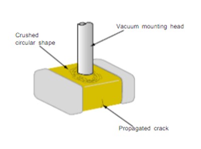
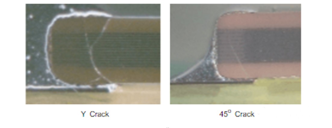
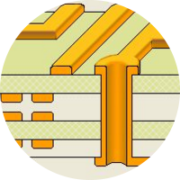
Typical bending crack
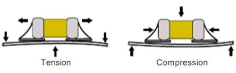
The ceramic body of the MLCC does not bend with the PCB and is therefore subject to tensile stress, see figure below. Ceramic materials are highly compressible but weakly stretchable. Cracks occur when the tensile force is greater than the inherent material strength.
Common stress sources include: operation in the PCB SMT assembly process; people, equipment, gravity and other factors in the flow process; through-hole (THT) component insertion; PCBA testing, PCBA board segmentation (v-cut or milling cutter sub-board) ); printed circuit board installation; PCB board positioning riveting; screw installation, etc.
① Factors producing mechanical stress:
A. Test probes cause PCB bending;
B. Exceeds the bending degree of the PCB and the rupture impact on the PCB;
C. Suction nozzle mounting (the pressure of the mounting nozzle is too large and the pressing distance is too deep) and the fixing of the centering claw will cause impact; when the product is mounted on the circuit board, it should not be subjected to excessive impact, and the suction must be regularly head and positioning jaws for inspection, repair and replacement;
E. Manual soldering process: During the soldering process, the soldering iron tip or anti-static tweezers press the device body, and the amount of solder on both ends of the device is excessive or uneven, which may cause cracking;
F. PCBA board cleaning: excessive manual cleaning force, wrong cleaning method or too hard cleaning brush head can cause cracks.
② Principle of mechanical stress crack generation:
The ceramic body of MLCC is a brittle material. If the PCB board is bent, it will be subjected to a certain amount of mechanical stress. When the stress exceeds the porcelain body strength of the MLCC, bending cracking occurs. Therefore, cracks caused by this bending only appear after welding.
A. The amount of stress received at different positions is different when the PCB board is bent: the component assembly is close to the PCBA board sub-board point;
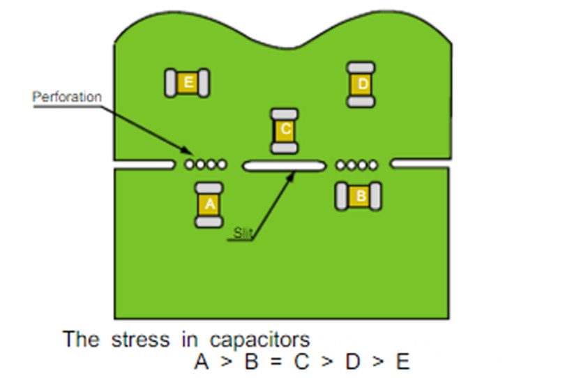
B. Cracking caused by bending of PCB board (product placement direction): cracking occurs when the product is close to or perpendicular to the splitting line;
C. Excessive amount of solder causes PCB board bending and cracking: Excessive amount of solder.
2.2 Internal factors: voids, cracks, delamination
(1) The main factors for voids in the ceramic medium are organic or inorganic pollution in the ceramic powder, improper control of the sintering process, etc. The generation of voids can easily lead to leakage, which in turn leads to local heating inside the device, which further reduces the insulating properties of the ceramic dielectric and leads to increased leakage. This process occurs cyclically and continues to deteriorate, leading to serious consequences such as cracking, explosion, and even burning of multilayer ceramic capacitors.
(2)Firing Crack often originates from one end of the electrode and expands in the vertical direction. The main reason is related to the cooling rate during sintering, and cracks and damage are similar to voids.
(3) Delamination. The sintering of multilayer ceramic capacitors (MLCC) is co-firing of multilayer material stacks. The sintering temperature can be as high as 1000°C or more. The weak bonding force between layers, the volatilization of internal pollutants during the sintering process, and the improper control of the sintering process may lead to the occurrence of delamination. The hazards of delamination are similar to those of voids and cracks, which are important inherent defects of multilayer ceramic capacitors.
