 Sign In
 Join Free
Top Blog

PCB Instant Quote
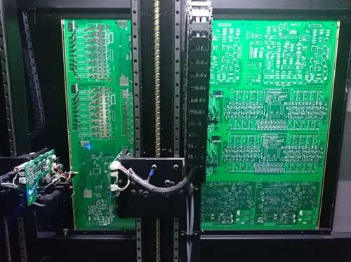
Different PCB layers Explanation
There are many types of PCB layers:
A. Signal Layers: The signal layers consist of Top Layer、Bottom Layer、Mid Layer 1……30. These layers are all layers with electrical connections, that is, the actual copper layer. The Mid layer refers to a middle layer for wiring.
B. Internal Plane: Internal Plane 1......16, These layers are generally connected to the ground and power supply. They also have the electrical connection function. They are also the actual copper layer, but the layer is generally not wiring, which is made up of the entire copper film.
C. Silkscreen Overlay: Include Top overlay and Bottom overlay. It is the symbols that are printed on the solder mask, such as component names, component symbols, component pins and copyright, etc., to facilitate future circuit soldering and troubleshooting.
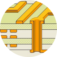
D. Paste Mask: Include Top paste and Bottom paste,It refers to the exposed surface mount pads that we can see, and the solder paste need to be coated before it is welded. Therefore, this layer is useful when hot air leveling and pcb stencil are made.
(Paste Mask)
E. Solder Mask: Include Top solder and Bottom solder, It is the opposite of the solder paste, referring to the cover of green oil layer. The layer does not stick solder to prevent the short circuiting of the excessive solder during welding. The solder coating covers the copper film and wire to avoid the copper oxidize in the air.
F. Mechanical Layers: It is generally used to set up the size of the circuit board, the data mark, the alignment mark, the assembly description and other mechanical information. This information is different from the requirements of the design company or the PCB manufacturer.
G. Keep Out Layer: Define the boundary of the wiring layer. After defining the keep out layer, the wiring with electrical characteristics can not exceed the boundary of keep out layer.
H. Drill Layer: Include Drill guide and Drill drawing, they are drill datas.
F. Multi-layer: It refers to all PCB layers.
