 Sign In
 Join Free
Top Blog
PCB Instant Quote
Printed Circuit Board Design Choices
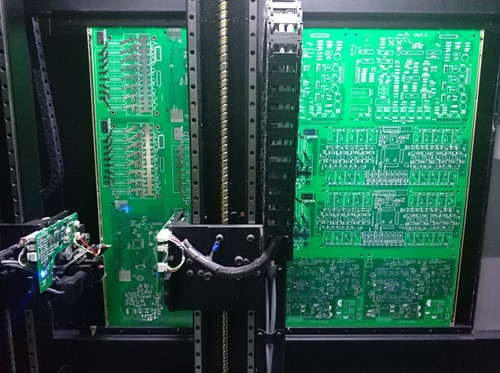
The bare PCB or printed circuit board is often the most expensive item on a PCB assembly bill of materials and can present a surprising number of choices for the design engineer. The basic composition is a substrate a conducting layer and a solder mask. The most common substrate known as Fr4 , it is rigid laminate composite of woven fiberglass and a flame-retardant epoxy. It’s a good general-purpose substrate due to its excellent strength-to-weight ratio dimensional stability and relatively low cost. There are number of other options including high temperature polyimide for transportation and high-temperature environments and materials for high frequency designs. But today we’ll focus on FR4. There are still at least four variables for the engineer and PCB designer to evaluate.
First is thickness. Fr4 boards can be as thin as 0.008inches to as thick as 0.125inches. The standard thickness is 0.062 inches or 1/16 of an inch think. If you are very concerned about the weight of your final product, you can get 0.031, half as thick, for about the same price.For large boards, you might want a thicker substrate for increase rigidity.
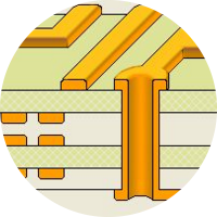
The second variable is thickness of the conducting layer. This is specified as copper weight or ounces of copper per square foot of board. You can see copper layer under the solder mask layer. The standard is one ounce about1.4 thousandths of an inch thick or about one-third as thick as a sheet of copy paper. Boards with half ounce to eight ounces are readily available. The thicker the copper layer the more current you will be able to run through the traces. The trace off is that the traces will need to have a coarse pitch and you won’t be able to use the smallest ICS with their closely spaced pins. You’ll have to specify larger components.
The third variable is layer count. The most common is 2 layers. One on top and one on bottom,but we also design and manufacture a lot of single layer boards as well as muti-layer boards with up to 24 layers of copper sandwich between the layers of FR4. Each additional set of layers increases the materials cost of the bare board but makes it easier to lay out the design and achieve high component density. Since there is no impact on manufacturing cost, the trade-off can make sense when small board size is important.
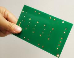
Finally the fourth variable is color of the solder mask layer. The green is the most familiar, but for a little more money you can get red black blue and white including a non yellowing white for boards with LEDs to reflect the LED’s true color without changing it. Some companies use color to differentiate prototype boards from the final product and others use color as part of their branding.
Contact us to learn more about our PCB service at service@pcbbee.com.
