 Sign In
 Join Free
Top Blog
PCB Instant Quote
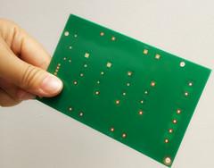
Detailed explanation of three common drilling holes in PCB
Let's introduce the common drilling holes in PCB: through hole, blind hole and buried hole.
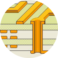
The plated through hole (VIA), a common hole, is used for conducting or connecting copper foil lines between conductive patterns in different layers of circuit boards. For example (such as blind holes, buried holes), but can not insert components. Because PCB is formed by stacking and accumulating many copper foil layers, each layer of copper foil will be covered with an insulating layer, so that the copper foil layers can not communicate with each other, and its signal link depends on via.
The characteristics are: in order to meet the needs of customers, the through holes of PCB must be plugged. With the rapid development of electronic industry, the technology of PCB fabrication and surface mounting has been put forward higher requirements. The technology of plugging through hole is applied, and the following requirements should be met: 1. the through hole has copper, solder mask can be or not plugged. 2. Tin and lead must be present in the through hole. There is a certain thickness requirement (4um) that no solder mask ink should be allowed to enter the hole, resulting in tin beads hidden in the hole. 3. Plated through holes must have solder mask ink plugged, no light transmission, no tin rings, and leveling requirements.
Blind hole: The outermost circuit layer in PCB is connected with the adjacent inner layer by plated hole, because the opposite can not be seen, so it is called Blind Pass. At the same time, in order to increase the space utilization between PCB layers, blind holes are applied.
Features: Blind holes are located on the top and bottom of circuit boards, and have a certain depth. They are used for linking the surface circuit layer and the underlying inner circuit layer. The depth of holes usually does not exceed a certain ratio (aperture). This production method needs to pay special attention to the depth of drilling (Z axis) to be just right, if not pay attention to it will cause difficulties in electroplating in the hole, so almost no factory can adopt it. It can also drill the hole first when the circuit layer needs to be connected in advance, and then bond it together, but it needs more precise positioning and alignment device.
Buried hole is the connection between any circuit layers in PCB, but it does not lead to the outer layer. It also means the through hole that does not extend to the surface of PCB.
Features: This process can not be achieved by bonding after drilling, drilling must be performed at the time of individual circuit layers, first local bonding after the first plating treatment, and finally all bonding, more time than the through hole and blind hole, so the PCB price is the most expensive. This process is usually used only for high-density circuit boards to increase the usability of other circuit layers.
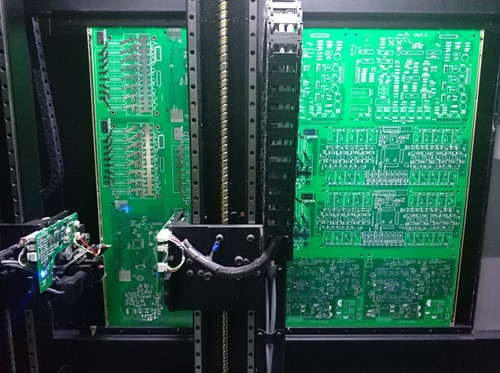
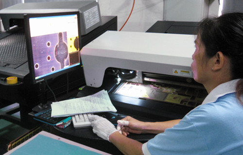
In PCB production process, drilling is very important, not sloppy. Because drilling is to drill the required holes in the copper clad laminate to provide electrical connection and fix the the device. If the operation is inappropriate, there is a problem in the process of through holes, the device can not be fixed on the circuit board, which will affect the use of the PCB board, and the whole board will be scrapped, so the drilling process is very important.
