 Sign In
 Join Free
Top Blog
PCB Instant Quote
Classification and selection of PCB materials
1. The FR-4 we often choose is not the name of a PCB material.
We often refer to the "FR-4" is a kind of flame resistance material grade code, it represents that the resin material must be extinguished by itself after the combustion, it is not a material name, but a material level. FR-4 grade materials used on the circuit board are many kinds, but most are based on a composite made of the so-called Tera-Function epoxy resin plus a filler (Filler) and a glass fiber. When you choose the printed circuit board material, you must know what the characteristic you need to meet.
There are two main types of PCB substrates: organic substrate materials and inorganic substrate materials, and the most used are organic substrate materials. Different layers use different PCB base materials, for example, 3~4 laminates should be made of prefabricated composite materials, and double sided PCB use glass epoxy resin material.
2. Consider the impact of SMT before selecting the pcb sheet material.
In the process of lead-free electronic assembly, due to the increase of temperature, the degree of bending of printed circuit boards is increasing. Therefore, in SMT, it is required to use small bending plates, such as FR-4. Due to the influence of expansion and contraction stress on components after heating, it will cause electrode stripping and reduce reliability. Therefore, we should pay attention to material expansion coefficient when selecting pcb material, especially when components are greater than 3.2 * 1.6mm. SMT technology requires PCB board have high thermal conductivity, excellent heat resistance ( 150℃, 60min) and weldability (at 260℃, 10s), high bonding strength of copper foil (1.5 x 10⁴Pa) and flexural strength (25 * 104Pa), high conductivity and low dielectric constant, good blanking (accuracy + 0.02mm) and detergent compatibility. In addition, it requires be smooth appearance, no warping, no cracks, no scars and no rust etc..
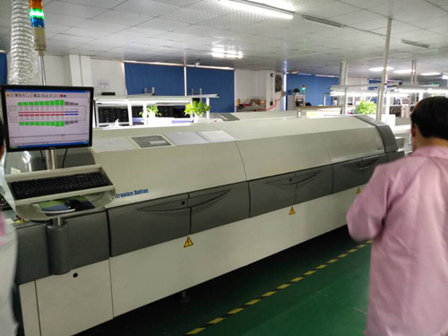
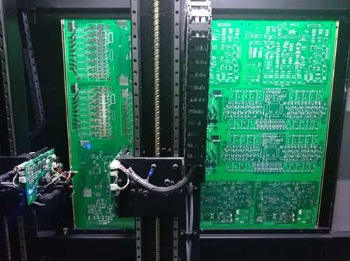
(SMT Line)
3. The thickness selection of PCB material
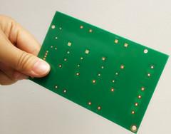
The thickness of printed circuit boards is 0.5mm, 0.7mm, 0.8mm, 1mm, 1.5mm, 1.6mm, (1.8mm), 2.7mm, (3.0mm), 3.2mm, 4.0mm,6.4mm. 0.7mm & 1.5mm is used for the design of double-sided PCB with gold fingers. From the point of view of production, the smallest single board should not be less than 250 * 200mm, and the ideal size is (250 to 350mm) x (200 * 250mm). For the long edge less than 125mm or the wide edge less than 100mm PCB, it is easy to use the way of panel. The surface mount technology of thickness 1.6mm substrate bending is specified on the warpage of less than 0.5mm, less than 1.2mm under warping. Usually the allowable bending rate is less than 0.065%. According to the metal material, it can be divided into 3 kinds. According to the structure rigid and soft, it can be divided into 3 kinds. The electronic through hole components is also developing to the high foot number, the miniaturization, the SMD and the complication. The electronic through hole components is mounted on the wiring board and welds the foot to the other side. This technology is called the THT (Through Hole Technology) insertion technique. So on the PCB board to drill holes for each foot, indicating the typical application of PCB.
4. Consider drilling before selecting the PCB material.
With the rapid development of SMT technology, multilayer PCB’s layers need to be connected, and it is realized by electroplating after drilling, which requires a variety of drilling equipment. In order to meet the above requirements, PCB numerical control drilling equipment with different properties is introduced at home and abroad. The production process of printed circuit board is a complex process, it involves a wide range. Mainly involved in the field of light chemistry, Electrochemistry and Thermochemistry; process steps involved in the manufacturing process is much more, with rigid multilayer circuit board as an example to illustrate the process. In the whole process, drilling is a very important step, hole processing time is the longest. And the position accuracy and quality of hole wall directly affect the Metallization of holes and SMT, also affect the PCB quality. The common method of drilling on the circuit board are CNC Mechanical drilling method and laser drilling method. At the present stage, the most frequently used method is mechanical drilling.

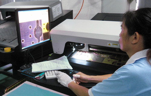
(CNC Drilling)
All in all, before selecting PCB material, we should consider the impact of SMT, the thickness and drilling etc.
